Contact Sales : 02 ) 6264 - 8600
English for Apparel Design Software only
HOME > 정보통 > 자료실
Fluorescence Microscopy: Getting the Picture Right
이름 : Optical Pioneer
2019-10-28 11:49:55 조회 :18260
Fluorescence Microscopy: Getting the Picture RightCamera choice has to strike a balance between certain sensor properties, camera-related topics, and the needs of the intended applications in industry or medicine. FELIX ASCHE, BASLER AG Fluorescence microscopy is a very broadly used term covering numerous applications. It ranges from basic life science applications such as time-lapse cell viability assays — in which dead cells are counted as they start to fluoresce by intrusion of a fluorochrome that cannot enter intact living cells — to sophisticated techniques where only very few photons or single molecules are detected and localized by specific high-end hardware and software. It can be quite complex to design an optical imaging system that perfectly fits a specific application. And at the same time, instrument manufacturers are facing pressure to keep the costs down in the medical and life sciences markets. Optical format and resolution Looking at the visible wavelength range, the optical setup considerations regarding format, magnification, and resolution do not significantly differ from normal light microscopy applications and are therefore not described here. However, it is important to know that the overall costs increase when larger optical formats such as the F-mount are used. The most common mount is the C-mount, which (with up to 1.1-in. sensors) delivers very good optical performance, as well as most products and solutions at a reasonable price. The smaller S-mount is a good choice when size-restricted and low-cost instruments are developed. Squared sensors are preferred to capture the maximum image content. Because the sensor takes over a central role in an imaging system, the selection regarding certain performance specifications is of major importance. CCD, CMOS, sCMOS, and BSI From its beginning in the late 1970s, CCD (charge-coupled device) technology has been strongly established and is still available in high-end microscopy cameras. Sony, the leading manufacturer of CCDs globally, has discontinued this technology, and instrument manufacturers using CCDs are being forced to find alternative cameras for their systems. The newer CMOS technology has spread through consumer sensor markets for many years and has recently become competitive. Noise levels are now comparable or even better than with the traditional and commonly used CCD sensors, enabling the new technology to deliver higher speed, higher resolution, and less power consumption/heat dissipation at lower prices into medical and life sciences applications. Scientific CMOS (sCMOS) cameras were introduced in 2010 through the collaboration of three companies working to provide better performance (mainly through faster CMOS-like readout speeds and higher dynamic range) compared to aging CCD technology, which continued to provide a superior noise behavior and brought higher image quality and sensitivity. CMOS sensor development is still rapidly accelerating. Recently, a technology called backside illumination (BSI) found its way into industrial image sensors. BSI significantly improves the pixels’ quantum efficiency. Coming from the smartphone market with its demand for smaller pixels, this technology involved reversing the orientation of the pixel structure to present the light-sensitive photodiode directly below the microlenses. With this design the metal wiring structures no longer inhibit the incident photons, improving the so-called fill factor (the relation of the photoactive and nonphotoactive area) of the pixels (Figure 1). 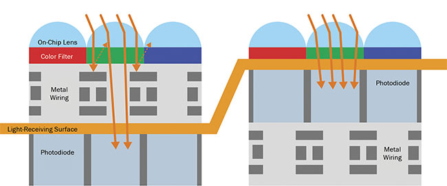 Figure 1. Frontside-illuminated (left) and backside-illuminated pixels (right). Courtesy of Basler AG. However, BSI sensors can have other additional noise sources contributing to the dark current. Dark current is the leakage of electrons during exposure. This can make these sensors less suitable for longer exposure times. Furthermore, state-of-the-art frontside-illuminated (FSI) sensors can still be a better choice in certain applications, showing excellent performance also in low-light conditions (Figure 2). 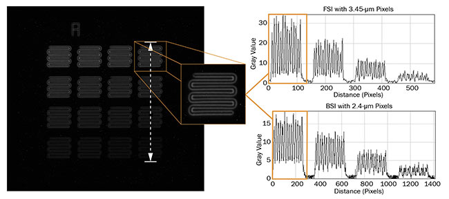 Figure 2. A persistent fluorescence carrier with 8.5-µm small structures of varying intensity was imaged under the same microscopic conditions (same optical path and lighting, and 10-s exposure) with a current BSI (Basler ace acA3088-57um, IMX178) and FSI sensor (Basler MED ace 5.1 MP, IMX250). For the FSI camera, the histogram shows nearly doubled gray values. Courtesy of Basler AG. Beyond CCD and CMOS, a few additional high-end sensor types are also on the market, such as EMCCD (electron multiplying CCD) and ICCD (intensified CCD). However, these cameras are generally not considered for large products today, as the technology is too expensive and serves mostly niche applications. CMOS technology will continue to evolve in the years to come; fluorescence microscopy can be expected to be dominated by this state-of-the-art technology in the future, while further developments of traditional CCD technology will tail off. For instrument manufacturers and their current and future products, cameras with CMOS sensors are acknowledged as the better choice. For more details: please click the link below. https://www.photonics.com/Articles/Fluorescence_Microscopy_Getting_the_Picture_Right/a65127 |
